


Disclaimer : Since this vulnerability has been made public, here is a small blog post explaining the methodology we used to find and exploit the same vulnerability.
Recap
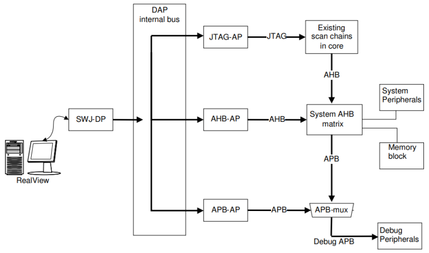
In the first part of this series, we explained the basics of the debug interface available on ARM chips. Basically, the external debugger talks using the SWD protocol to the Debug Port (DP), which forwards requests to the different Access Ports (AP) available on the internal bus called the Debug Access Port (DAP). In the second part, we showed how access to the DAP allows to use the MEM-AP to access the whole memory space of the core (flash memory, peripherals, internal registers, …).
Since this interface allows retrieval of any information stored by the chip, it is quite difficult to protect any IP or secrets. Unfortunately, ARM does not provide a standard way to secure this interface so manufacturers implemented many different ways to restrict access to the DAP, sometimes with flaws in them.
Debug port protection failures
As an example, the nrf51family protection allows access to the DP and the MEM-AP, but only on specific memory regions. Some people found out that it was possible to read and write the CPU registers and step into the code. Using these features, they were able to locate a ldr instruction and instrument it to fetch the flash memory contents four bytes per four bytes.
Another example. On STM32 chips, the most common SWD interface protection is called Readout Protection (RDP). These protections differ amongst chip families, but we can sum up the following :
- RDP level 0 : No DAP protection
- RDP level 1 : DP and MEM-AP access is allowed, but MEM-AP can only fetch specific memory regions
- RDP level 2 : DP access is disabled
As we saw, in part two, some chips were vulnerable to a race condition, allowing to bypass the protection. There are other examples where the RDP protection was bypassed using glitches.
Here is another example : the nRF52840 uses a different mechanism called APPROTECT, which disables access to the MEM-AP when the APPROTECT register value is 0xFFFFFF00.

So what happens once this protection has been enabled ? Let’s have a look.
Mapping DAP bus
As previously seen, the DP SELECT register is used to address a specific AP on the bus. There can be up to 256 possible address values. We have also seen that the AP register 0xFC is usually the identification register (IDR). Using these, we can create a small script to query each AP for its IDR and see the results on the nRF52840 :
import pyHydrabus
s = pyHydrabus.SWD()

# Initialize the SWD interface and power up the debug power domain
s.bus_init()
s.read_dp(0)
s.write_dp(4, 0x10000000)

# Scan the DAP bus
for x in range(256):
    idcode = s.read_ap(x, 0xfc)
    if idcode != 0:
        print(f"{x:03d} - 0x{idcode:08x}")
000 - 0x24770011
001 - 0x02880000
There are two APs : the standard MEM-AP and the CTRL-AP, which is “a custom access port that enables control of the device when other access ports in the DAP are disabled by the access port protection.” It essentially allows to remove the protection (which erases the internal flash memory).
Once we enable the protection mechanism (through openOCD using the command “flash fillw 0x10001208 0x00 1“) the DP access is still present, but the previous script shows a different output :
000 - 0x23000000
001 - 0x02880000
Interestingly enough, all registers from the MEM-AP now return 0x23000000 instead of the correct value.
Attacking the AP protection
As we have seen, the DP does not seem to be affected by the protection, but the AP does. Looking at the Reset behavior of the chip, using the pin reset is enough to reset the debug domain and is easily controllable from an external signal. This also has the advantage of keeping the internal power regulators up so the boot time is more consistent.
Being able to query the MEM-AP IDR at a lower level to know if the device is protected or not also helps speeding up the campaign. That way, fewer SWD packets need to be sent to the target in order to validate if the attack was successful or not.
As such, a well timed voltage glitch could alter the register comparison, and keep the MEM-AP enabled despite the APPROTECT register being set. We now have our plan to perform the attack :
- Keep the target under reset by keeping the reset pin (P0.18) low
- Raise the reset pin. This will start the target boot process
- After a certain delay, inject the glitch
- Connect on the SWD bus, and query the MEM-AP IDR
- If IDR ==
0x23000000goto1. If IDR ==0x24770011goto6 - Profit
I won’t get into the glitching details, as we used the same crowbar technique used in the original disclosure (I highly recommend reading this article) and the results are similar.
Conclusions
In this post, we presented some mechanisms implemented by manufacturers to protect access to the debug interface of their chips. These mechanisms do sometimes suffer from logical flaws, but most of the times are vulnerable to glitches. While these protections are helpful as a first barrier, they would never prevent a determined attacker from gaining access to the contents of the chip.
Knowing the inner working of the protocols involved also help a lot when building glitch campaigns. Not only will it give you a deeper understanding of the way things work, but it will also give you a broader range of information available about your target.
We also need to emphasize that none of these general purpose chips provide any protection against fault attacks. What they offer is a “best effort” type of protection, but you should not rely on them to protect keys or IP. Should you need such kind of protection, have a look at secure elements which are specifically made to protect critical assets.
